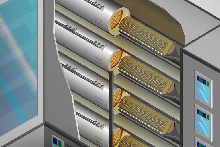
Widely embraced in the semiconductor industry, LPCVD finds applications in depositing materials like silicon nitride, silicon dioxide, and polysilicon. Its controlled nature and ability to achieve precise thickness and uniformity make LPCVD a cornerstone in the creation of advanced semiconductor devices. Operating at lower pressures compared to other chemical vapor deposition methods, LPCVD ensures meticulous control over film properties.
The process in short
The process initiates with the introduction of carefully chosen precursor gases into a vacuum chamber, where controlled chemical reactions occur at low pressures and temperatures. These reactions result in a thin film layer deposition onto the silicon wafer's surface. The growth rate and uniformity of the film are precisely regulated, offering a level of control essential for fabricating semiconductor devices with specific electrical or structural characteristics.
Top-notch solutions backed by expert support
 Tyke Johnson, Product Line Manager, Kanthal.The LPCVD processes are critical in ensuring that semiconductor devices have consistent material purity, which helps prevent defects that could negatively impact their electrical, structural, and thermal properties. These devices are highly sensitive to variations, making it essential to meet or exceed industry standards in LPCVD processes, ensuring that electronic components are reliable, high-performing, and long-lasting. Moreover, it's crucial to maintain control over chemical reactions in the vacuum environment, as any deviation in LPCVD parameters can lead to unintended reactions, highlighting the need for strict quality control in these processes.
“Our reputation for excellence has made us a trusted brand in both the semiconductor and industrial heating industries. Our products are widely used worldwide, and we are also proud to offer our customers dedicated technical support from our expert team,” says Tyke Johnson, Product Line Manager at Kanthal. “Kanthal’s approach is rooted in years of experience and guided by lean manufacturing principles. As a result, we can deliver top-notch products that meet the rigorous standards of our customers.”
Our commitment to delivering high-quality heating solutions to our customers is unwavering.
“At Kanthal, our topmost priority is quality. We ensure consistency through in-process checks, customized packaging for safe transport, and meticulous documentation. Our commitment to delivering high-quality heating solutions to our customers is unwavering. For us, it's about reliability, expertise, and a promise to deliver excellence,” Johnson adds.
Several crucial materials can be deposited through LPCVD, each serving specific purposes in semiconductor device fabrication:
Polysilicon:
PLPCVD is commonly employed for depositing polysilicon (polycrystalline silicon) thin films onto silicon wafers. In this process, precursor gases containing silicon are introduced into a vacuum chamber, leading to controlled chemical reactions that result in the deposition of a polysilicon layer on the wafer's surface.
Polysilicon is widely used in the fabrication of semiconductor devices, particularly in the manufacturing of thin-film transistors (TFTs) and as a gate material in integrated circuits.
Nitride:
LPCVD is also employed for the deposition of nitride thin films, often silicon nitride (Si3N4). Nitride deposition involves the controlled reaction of nitrogen-containing precursor gases with silicon-based precursors in a low-pressure environment.
Silicon nitride films serve as insulating layers, diffusion barriers, and protective coatings in semiconductor devices. They are integral in enhancing the reliability and performance of electronic components.
Doped Polysilicon:
Doped polysilicon deposition through LPCVD involves introducing precursor gases containing both silicon and dopant elements into a vacuum chamber. The resulting chemical reactions deposit a polysilicon layer with controlled dopant concentrations on the wafer's surface.
Doped polysilicon is utilized in various semiconductor applications, including the formation of resistors, capacitors, and other components requiring precise control over electrical conductivity.
In essence, LPCVD enables the controlled deposition of materials contributing to semiconductor devices' intricate architecture and functionality. These processes showcase the versatility of LPCVD in tailoring the material properties essential for the diverse components integrated into modern electronic circuits.
Previously supplied under the MRL and Sandvik Materials Technology brands, our Fibrothal® heating elements are also known as Aztec, Helix, Black Max, or Magna SW in North America and White John in Europe.
Read more
Our latest articles